SBC In-System Programming: Information | VisISP-52 ISP Application
SBCMON Monitor/Operating System: Main Page | Manual
SBCMON-based Software: SBCMON Monitor | Keypad Demo | LCD Echo Demo | Hardware Clock | Software Clock
SBCMON-based PS/2 Software: PS/2 Comm Monitor | PS/2 Keyboard | PS/2 Mouse
ORDER 8052.com SBC: PCB, KIT OR BUILT SBC AVAILABLE FOR PURCHASE
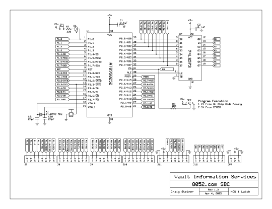
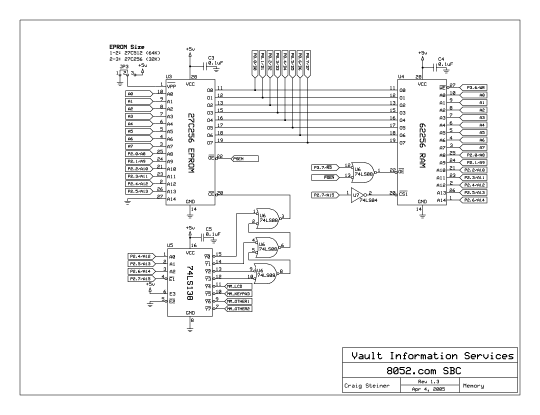
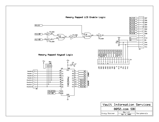
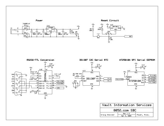
This page includes the schematics for the 8052.com SBC. You may build a functioning version of the SBC by building based on these schematics. Click on each schematic page for a full-size version.
Microcontroller & Memory Latch
Memory (RAM & EPROM)
Memory-Mapped LCD & Keypad
Power & Misc.
In-System Programming (ISP) Schematic
Bill of Materials
The following parts are needed to build the 8052.com SBC described above:
| Reference | Quantity | Part | Digikey Part Number | Datasheet |
| C1-C14,C24,C25 | 16 | 0.1uF ceramic capacitor | 1338PH-ND | |
| C15,C23 | 2 | 10uF electrolytic capacitor | P5134-ND | |
| C16-C19 | 4 | 1uF electrolytic capacitor | P10312-ND | |
| C20,C21 | 2 | 27pF ceramic capacitor | P10797-ND | |
| C22 | 1 | 1000uF electrolytic capacitor | P10253-ND | |
| C26 | 1 | 100uF capacitor | P11198-ND | |
| D1-D4 | 4 | 1N4001 diode | 1N4001GICT-ND | |
| D5 | 1 | Red LED | 404-1090-ND | |
| D6 | 1 | Yellow LED | 404-1092-ND | |
| J1 | 1 | 2.1mm power connector | CP-202A-ND/CP-102AH-ND | |
| J2 | 1 | DB25 male conector | A23285-ND | |
| J3,J4 | 2 | 14-pin Female Header | S4207-ND | |
| J5 | 1 | 8-pin Female Header | S4008-ND | |
| J6 | 1 | DB6 DB9 female RS232 | A23303-ND | |
| J7-J12 | 6 | 8-pin SIPs | ||
| JP1 | 1 | 2-pin jumper | ||
| JP2-JP6 | 5 | 3-pin jumper | ||
| R1,R7 | 2 | 330 | P330BACT-ND | |
| R2 | 1 | 220 | P220BACT-ND | |
| R3 | 1 | 10K Variable Resistor | 3362U-103-ND | |
| R5,R6,R8 | 3 | 10K | P10KBACT-ND | |
| R4 | 1 | 100 | P100BACT-ND | |
| RN1 | 1 | 6.8k 6-pin resistor network | 750-61-R6.8K-ND | |
| SW1,SW2 | 2 | Momentary push button, normally open | P8006S-ND | |
| U1 | 1 | Atmel AT89S8253 | AT89S8253-24PI-ND | Datasheet |
| U2 | 1 | 74LS573 octal latch | 296-1596-5-ND or TC74HC573AP-ND | Datasheet |
| U3 | 1 | 27C64 UV EPROM (optional) | 497-1685-5-ND | Datasheet |
| U4 | 1 | 62256 8x32k RAM (or 6264) | 428-1080-ND | Datasheet |
| U5 | 1 | 74LS138 3x8 decoder/MUX | 296-1639-5-ND | Datasheet |
| U6 | 1 | 74LS08 Quad 2-Input AND Gate | 296-1633-5-ND | Datasheet |
| U7 | 1 | 74LS04 Hex Inverter | 296-1629-5-ND | Datasheet |
| U8 | 1 | 74LS32 Quad 2-Input OR Gate | 296-1658-5-ND | Datasheet |
| U9 | 1 | 74HC541 Octal Buffer/Driver | 296-12813-5-ND | Datasheet |
| U10 | 1 | MAX232 Dual RS232 Driver/Receiver | 296-1402-5-ND | Datasheet |
| U11 | 1 | 74LS125 Quad Tri-State Buffer Active Low | 296-1638-5-ND or 296-8386-5-ND | Datasheet |
| U12 | 1 | 74HC126 Quad Tri-State Buffer Active High | 296-8221-5-ND | Datasheet |
| U13 | 1 | DS1307 real time clock (RTC) | DS1307-ND | Datasheet |
| U14 | 1 | AT25010A 128x8 Serial EEPROM | AT25010A-10PI-2.7-ND | Datasheet |
| U15 | 1 | (OMIT--Don't use) MN13811 4.6V Reset Supervisor | Datasheet | |
| U16 | 1 | LM7805 5V voltage regulator | 296-1974-5-ND | Datasheet |
| X1 | 1 | 11.0592 MHz crystal | X139-ND | |
| X2 | 1 | 32.768 kHz crystal | 300-1002-ND | |
| 1 | 40-pin IC Socket | A9440-ND | ||
| 2 | 28-pin IC Socket | A9428-ND | ||
| 2 | 20-pin IC Socket | A9420-ND | ||
| 2 | 16-pin IC Socket | A9416-ND | ||
| 5 | 14-pin IC Socket | A9414-ND | ||
| 2 | 8-pin IC Socket | A9408-ND | ||
| 3 | 36-pin breakaway headers for J7-J12, JP1-JP6 | WM6436-ND | ||
| 1 | 16x2 LCD (left side 2x7 connector) | 67-1770-ND or 67-1780-ND |
||
| 1 | 4x4 Keypad | GH5003-ND | ||
| 1 | 5W Heatsink for 7805 | HS121-ND | ||
| 1 | Wall transformer, 12VAC 750MA, 2.1mm | MT7119-ND | ||
| 4 | Bumpons Hemispheres .50X.14 Clear | SJ5312-7-ND |
TROUBLESHOOTING
This is a list of potential solutions to problems that have been observed when constructing the SBC.
Problem: Everything works, but memory-mapped LCD hangs on 'M0I' command with LCD attached to J3.
LCD does work when attached to J4 (direct-connect) and keypad and RAM also work.
Solution: Check pin 1 of U5 ('138).


