


The 8051 has three very general types of memory. To effectively program the 8051 it is necessary to have a basic understanding of these memory types.
The memory types are illustrated in the following graphic. They are: On-Chip Memory, External Code Memory, and External RAM.
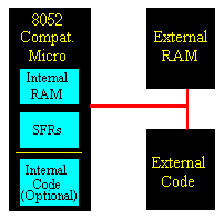
On-Chip Memory refers to any memory (Code, RAM, or other) that physically exists on the microcontroller itself. On-chip memory can be of several types, but we'll get into that shortly.
External Code Memory is code (or program) memory that resides off-chip. This is often in the form of an external EPROM.
External RAM is RAM memory that resides off-chip. This is often in the form of standard static RAM or flash RAM.
Code memory is the memory that holds the actual 8051 program that is to be run. This memory is limited to 64K and comes in many shapes and sizes: Code memory may be found on-chip, either burned into the microcontroller as ROM or EPROM. Code may also be stored completely off-chip in an external ROM or, more commonly, an external EPROM. Flash RAM is also another popular method of storing a program. Various combinations of these memory types may also be used--that is to say, it is possible to have 4K of code memory on-chip and 64k of code memory off-chip in an EPROM.
When the program is stored on-chip the 64K maximum is often reduced to 4k, 8k, or 16k. This varies depending on the version of the chip that is being used. Each version offers specific capabilities and one of the distinguishing factors from chip to chip is how much ROM/EPROM space the chip has.
However, code memory is most commonly implemented as off-chip EPROM. This is especially true in low-cost development systems and in systems developed by students.
Programming Tip: Since code memory is restricted to 64K, 8051 programs are limited to 64K. Some assemblers and compilers offer ways to get around this limit when used with specially wired hardware. However, without such special compilers and hardware, programs are limited to 64K.
External RAMAs an obvious opposite of Internal RAM, the 8051 also supports what is called External RAM.
As the name suggests, External RAM is any random access memory which is found off-chip. Since the memory is off-chip it is not as flexible in terms of accessing, and is also slower. For example, to increment an Internal RAM location by 1 requires only 1 instruction and 1 instruction cycle. To increment a 1-byte value stored in External RAM requires 4 instructions and 7 instruction cycles. In this case, external memory is 7 times slower!
What External RAM loses in speed and flexibility it gains in quantity. While Internal RAM is limited to 128 bytes (256 bytes with an 8052), the 8051 supports External RAM up to 64K.
Programming Tip: The 8051 may only address 64k of RAM. To expand RAM beyond this limit requires programming and hardware tricks. You may have to do this "by hand" since many compilers and assemblers, while providing support for programs in excess of 64k, do not support more than 64k of RAM. This is rather strange since it has been my experience that programs can usually fit in 64k but often RAM is what is lacking. Thus if you need more than 64k of RAM, check to see if your compiler supports it-- but if it doesn't, be prepared to do it by hand.
On-Chip MemoryAs mentioned at the beginning of this chapter, the 8051 includes a certain amount of on-chip memory. On-chip memory is really one of two types: Internal RAM and Special Function Register (SFR) memory. The layout of the 8051's internal memory is presented in the following memory map:
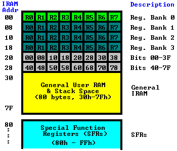
As is illustrated in this map, the 8051 has a bank of 128 bytes of Internal RAM. This Internal RAM is found on-chip on the 8051 so it is the fastest RAM available, and it is also the most flexible in terms of reading, writing, and modifying its contents. Internal RAM is volatile, so when the 8051 is reset this memory is cleared.
The 128 bytes of internal ram is subdivided as shown on the memory map. The first 8 bytes (00h - 07h) are "register bank 0". By manipulating certain SFRs, a program may choose to use register banks 1, 2, or 3. These alternative register banks are located in internal RAM in addresses 08h through 1Fh. We'll discuss "register banks" more in a later chapter. For now it is sufficient to know that they "live" and are part of internal RAM.
Bit Memory also lives and is part of internal RAM. We'll talk more about bit memory very shortly, but for now just keep in mind that bit memory actually resides in internal RAM, from addresses 20h through 2Fh.
The 80 bytes remaining of Internal RAM, from addresses 30h through 7Fh, may be used by user variables that need to be accessed frequently or at high-speed. This area is also utilized by the microcontroller as a storage area for the operating stack. This fact severely limits the 8051s stack since, as illustrated in the memory map, the area reserved for the stack is only 80 bytes--and usually it is less since this 80 bytes has to be shared between the stack and user variables.
The 8051 uses 8 "R" registers which are used in many of its instructions. These "R" registers are numbered from 0 through 7 (R0, R1, R2, R3, R4, R5, R6, and R7). These registers are generally used to assist in manipulating values and moving data from one memory location to another. For example, to add the value of R4 to the Accumulator, we would execute the following instruction:
-
ADD A,R4
Thus if the Accumulator (A) contained the value 6 and R4 contained the value 3, the Accumulator would contain the value 9 after this instruction was executed.
However, as the memory map shows, the "R" Register R4 is really part of Internal RAM. Specifically, R4 is address 04h. This can be see in the bright green section of the memory map. Thus the above instruction accomplishes the same thing as the following operation:
-
ADD A,04h
But watch out! As the memory map shows, the 8051 has four distinct register banks. When the 8051 is first booted up, register bank 0 (addresses 00h through 07h) is used by default. However, your program may instruct the 8051 to use one of the alternate register banks; i.e., register banks 1, 2, or 3. In this case, R4 will no longer be the same as Internal RAM address 04h. For example, if your program instructs the 8051 to use register bank 3, "R" register R4 will now be synonomous with Internal RAM address 1Ch.
The concept of register banks adds a great level of flexibility to the 8051, especially when dealing with interrupts (we'll talk about interrupts later). However, always remember that the register banks really reside in the first 32 bytes of Internal RAM.
Programming Tip: If you only use the first register bank (i.e. bank 0), you may use Internal RAM locations 08h through 1Fh for your own use. But if you plan to use register banks 1, 2, or 3, be very careful about using addresses below 20h as you may end up overwriting the value of your "R" registers!
Bit MemoryThe 8051, being a communications-oriented microcontroller, gives the user the ability to access a number of bit variables. These variables may be either 1 or 0.
There are 128 bit variables available to the user, numberd 00h through 7Fh. The user may make use of these variables with commands such as SETB and CLR. For example, to set bit number 24 (hex) to 1 you would execute the instruction:
- SETB 24h
- MOV 20h,#0FFh
is equivalent to:
SETB 00h
SETB 01h
SETB 02h
SETB 03h
SETB 04h
SETB 05h
SETB 06h
SETB 07h
Programming Tip: If your program does not use bit variables, you may use Internal RAM locations 20h through 2Fh for your own use. But if you plan to use bit variables, be very careful about using addresses from 20h through 2Fh as you may end up overwriting the value of your bits!
Bit variables 00h through 7Fh are for user-defined functions in their programs. However, bit variables 80h and above are actually used to access certain SFRs on a bit-by-bit basis. For example, if output lines P0.0 through P0.7 are all clear (0) and you want to turn on the P0.0 output line you may either execute:
- MOV P0,#01h
or you may execute:
SETB 80h
Both these instructions accomplish the same thing. However, using the SETB command will turn on the P0.0 line without effecting the status of any of the other P0 output lines. The MOV command effectively turns off all the other output lines which, in some cases, may not be acceptable.
Programming Tip: By default, the 8051 initializes the Stack Pointer (SP) to 07h when the microcontroller is booted. This means that the stack will start at address 08h and expand upwards. If you will be using the alternate register banks (banks 1, 2 or 3) you must initialize the stack pointer to an address above the highest register bank you will be using, otherwise the stack will overwrite your alternate register banks. Similarly, if you will be using bit variables it is usually a good idea to initialize the stack pointer to some value greater than 2Fh to guarantee that your bit variables are protected from the stack.
Special Function Register (SFR) MemorySpecial Function Registers (SFRs) are areas of memory that control specific functionality of the 8051 processor. For example, four SFRs permit access to the 8051s 32 input/output lines. Another SFR allows a program to read or write to the 8051s serial port. Other SFRs allow the user to set the serial baud rate, control and access timers, and configure the 8051s interrupt system.
When programming, SFRs have the illusion of being Internal Memory. For example, if you want to write the value "1" to Internal RAM location 50 hex you would execute the instruction:
- MOV 50h,#01h
Similarly, if you want to write the value "1" to the 8051s serial port you would write this value to the SBUF SFR, which has an SFR address of 99 Hex. Thus, to write the value "1" to the serial port you would execute the instruction:
- MOV 99h,#01h
As you can see, it appears that the SFR is part of Internal Memory. This is not the case. When using this method of memory access (its called direct address), any instruction that has an address of 00h through 7Fh refers to an Internal RAM memory address; any instruction with an address of 80h through FFh refers to an SFR control register.
Programming Tip: SFRs are used to control the way the 8051 functions. Each SFR has a specific purpose and format which will be discussed later. Not all addresses above 80h are assigned to SFRs. However, this area may NOT be used as additional RAM memory even if a given address has not been assigned to an SFR.
| Previous: Introduction | Tutorial Contents | Next: Special Function Registers (SFRs) |